Product Details
- Wide flat performance IF BW
- Wide RF and LO BWs (~ 1.6GHz)
- Ideal for multi-carrier systems
- Drives ADC directly
- Ultra-linear +41dBm IP3O
- Low noise figure
- Excellent ACLR performance
- 200Ω output impedance
- Fully integrated DPD demodulator
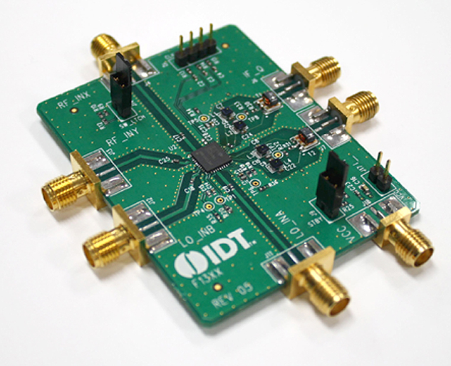
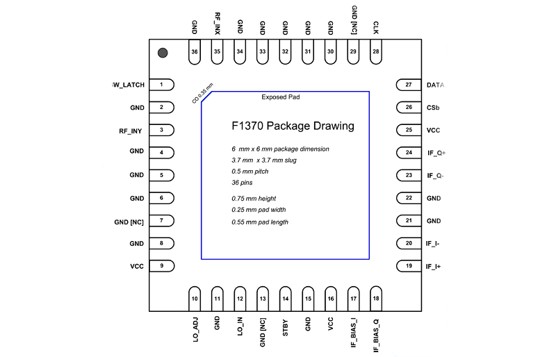
- 6mm x 6mm 36-pin package
- Standby mode with fast recovery
- ICC: 275mA
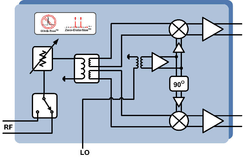
The F1370 is a highly linear complex IF digital pre-distortion (DPD) demodulator with a built-in digital step attenuator (DSA) and single-pole double-throw switches (SP2Ts). It receives the signal coming out of the PA so that the I&Q data at the baseband can be pre-distorted before being sent to the Tx DAC to counteract the distortion inherent in the downstream PA. The signal coupled from the PA is adjusted via a DSA to a lower level and then sub-sampled at an IF frequency of ~200MHz which necessitates the need for a highly linear demodulator to downmix to quadrature IF from the Transmit frequency. By sampling IF_I and IF_Q independently and then digitally combining these signals, an effective doubling of the sample rate can be achieved. Any distortion in this path will degrade the performance of the DPD algorithm. By utilizing an ultra-linear demodulator with integrated DSA such as the F1320, the ACLR and/or power consumption of the full Tx system can be improved significantly.