Product Details
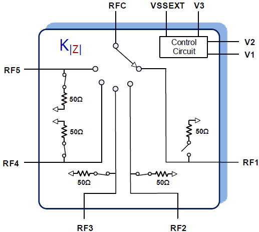
- Five symmetric broadband, absorptive RF ports
- Constant Impedance, Kz, feature
- High-performance RF
- Isolation of 50dB at 2700MHz
- Insertion Loss of 1.2dB at 2700MHz
- High continuous RF CW power handling
- Selected RF path: 33dBm
- Terminated RF path: 27dBm
- High linearity:
- IIP2 of 114dBm
- IIP3 of 60dBm
- Single 2.7V to 5.50V supply voltage
- External Negative Supply Option
- 3.3V and 1.8V compatible control logic
- Operating temperature -40 °C to +105 °C
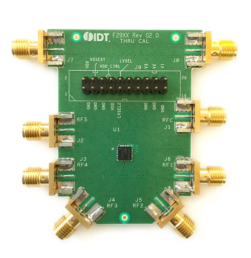
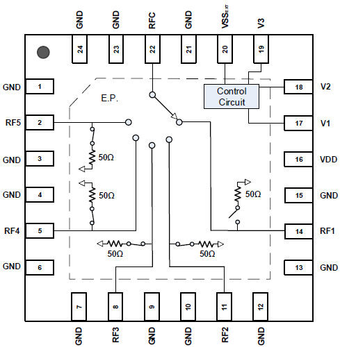
- 4mm x 4mm 24-pin QFN package
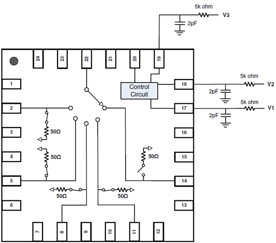
The F2915 is a high reliability, low insertion loss, 50Ω SP5T absorptive RF switch designed for a wide range of wireless and other RF applications. This device covers a broad frequency range from 50MHz to 8000MHz. In addition to providing low insertion loss, the F2915 also delivers excellent linearity and isolation performance while providing a 50Ω termination to the unused RF ports. The F2915 also includes a patent-pending constant impedance (Kz) feature. Kz improves hot switching ruggedness, minimizes LO pulling in VCOs, and reduces phase and amplitude variations in distribution networks. It is also ideal for dynamic switching/selection between two or more amplifiers while avoiding damage to upstream/downstream sensitive devices such as PAs and ADCs.
The F2915 uses a single positive supply voltage supporting three logic control pins using either 3.3V or 1.8V control logic. Connecting a negative voltage to pin 20 disables the internal negative voltage generator and becomes the negative supply.