Product Details
- RF Frequency Range: 0.6GHz to 2.7GHz
- Gain at 2.5GHz:
- 29.5dB typical max gain in non-bypass mode
- 10.9dB typical max gain in bypass mode
- DSA Control:
- DSA0: Single 6dB step via SPI/I3C control
- DSA1: Single 6dB step via 1-bit external pin control
- DSA2: 29dB range in 1dB steps via SPI/I3C control
- DSA3: 18dB range in 6dB steps via 2-bit external pin control
- +39dBm OIP3 at 2.5GHz
- NF at 2.5GHz
- 3.2dB typical in non-bypass mode
- 8.9dB typical in bypass mode
- +19.7dBm OP1dB at 2.5GHz
- ICC = 372mA
- Standby Mode for power savings with 9mA standby current
- 50Ω single-ended input/output impedances
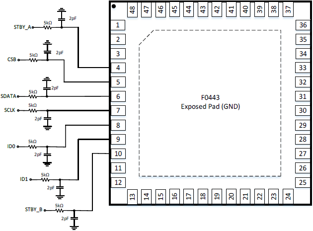
- 1.8V logic support
- Operating temperature range: -40 °C to +105 °C
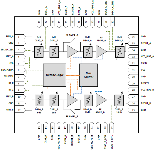
- 7mm × 7mm 48-LGA package
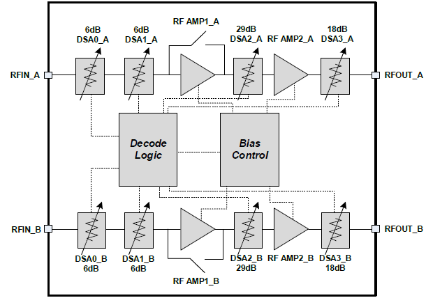
The F0443 is a highly integrated 0.6GHz to 2.7GHz dual-channel RF digital variable gain amplifier designed for use in diversity/MIMO receivers. The F0443 provides two independent receiver paths each with 29.5dB typical maximum gain and 3.2dB NF at 2.5GHz.
For each path, gain control is split into four separate digital step attenuators: DSA0 provides 6dB of attenuation in a single step using SPI/I3C control. Its counterpart, DSA1, also provides 6dB of attenuation in a single step but it is programmed instead using an external direct control pin. DSA2 yields 29dB of SPI/I3C-controlled attenuation in 1dB steps, while its counterpart, DSA3, includes 18dB attenuation in 6dB steps programmed via two external control pins. The device offers +39dBm nominal output IP3 at 2.5GHz using 372mA total ICC for two active paths with a +5V supply voltage.
The F0443 is packaged in a 7mm × 7mm, 48-LGA with 50Ω single-ended RF input and RF output impedances for easy integration into the signal path.
.jpg)