Product Details

- Gain at 3500MHz
- 34.5dB typical in High Gain Mode
- 28.5dB typical in Low Gain Mode
- 1.35dB NF at 3500MHz
- +23dBm OIP3 at 3500MHz
- OP1dB at 3500MHz
- +15dBm in High Gain Mode
- +14dBm in Low Gain Mode
- 50Ω single-ended input/output amplifier impedances
- IDD = 130mA
- Independent Standby Mode for power savings
- Supply voltage: +3.15V to +3.45V
- 5mm × 5mm, 32-LGA package
- -40 °C to +105 °C exposed pad operating temperature range
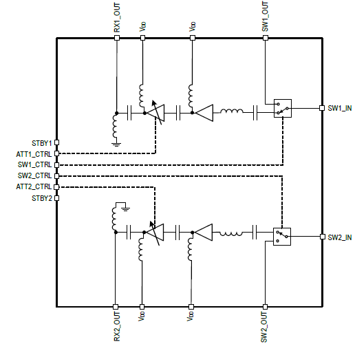
The F0453 is an integrated dual-path RF front-end consisting of an RF switch and two gain stages with 6dB gain control used in the analog front-end receiver of an Active Antenna System (AAS). The F0453 supports frequencies from 3400MHz to 3800MHz.
The F0453 provides 34.5dB gain with +23dBm OIP3, +15dBm output P1dB, and 1.35dB noise figure at 3500MHz. Gain is reduced 6dB in a single step with a maximum settling time of 31ns. The device uses a single 3.3V supply and 130mA of IDD.
The F0453 is offered in a 5mm x 5mm x 0.8mm, 32-LGA package with 50Ω input and output amplifier impedances for ease of integration into the signal path.
- Multi-mode, multi-carrier receivers
- 4.5G (LTE Advanced)
- 5G band 42 and 43
.jpg)