Product Details

- Independent dual-path operation
- RF output frequency: 450MHz to 2800MHz
- 18.3dB typical maximum gain (no attenuation)
- +31dBm OIP3 (no attenuation)
- +14dBm Output P1dB (no attenuation)
- 13dB NF corresponds to -142.5dBm/Hz output noise floor (no attenuation)
- Output noise floor -152.3dBm/Hz (VVA = 14dB, DSA = 1dB)
- Channel Isolation: 47dB
- DSA with 31dB total gain range in 1dB steps
- Multiple VVAs with 32dB gain range controlled by on-chip SPI controlled 11-bit DAC
- Variable Gain amplifier (VGA) is comprised of DSAs, VVAs, and a fixed-gain amplifier
- I lead Q by 90 degrees for high side LO injection
- Supports ZIF or CIF architectures
- Common-mode voltage range: +0.1V to +0.8V
- Integer-N and Fractional-N Synthesizer
- Direct 110Ω differential driven from I/Q DAC
- 50Ω single-ended RF output impedance
- Internal or external LO select
- +3.3V supply voltage at 685mA (LO_Out not turned on)
- Specified case temperature: -20°C to +115°C
- 10 × 10 mm, 68-VFQFPN package
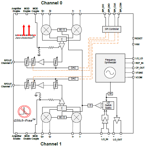
The F159V is a Dual-Path Integrated TRx IC that has an operating frequency range of 450MHz to 2800MHz. The device provides two independent transmit paths each with 18.3dB typical maximum gain with corresponding output noise floor of -142.5dBm/Hz, +31dBm OIP3, and +14dBm output P1dB designed to operate with a single +3.3V supply while consuming only 685mA DC current. Each signal path includes a quadrature modulator, voltage variable attenuator (VVA), digital step attenuator (DSA), and a fixed gain amplifier. The device supports a total of 32dB VVA adjustment range using a SPI-controlled 11-bit DAC, and each DSA has 31dB gain control range in 1dB steps using SPI control.
An on-chip frequency synthesizer is shared by both paths and is optimized for use in multi-carrier, multi-mode FDD and TDD base station transmitters achieving GSM-grade performance. The synthesizer offers both an integer mode and fractional mode. It requires an external loop filter and an external reference oscillator in the frequency range of 10MHz to 250MHz.
The F159V is packaged in a 10mm x 10mm, 68-pin QFN with 110Ω differential drive from external I/Q DACs and single-ended 50Ω RF output impedance for ease of integration into the signal-path lineup for each of the two transmitter paths. Each path has independent power supply control thereby allowing optimum power efficiency.
.PNG)