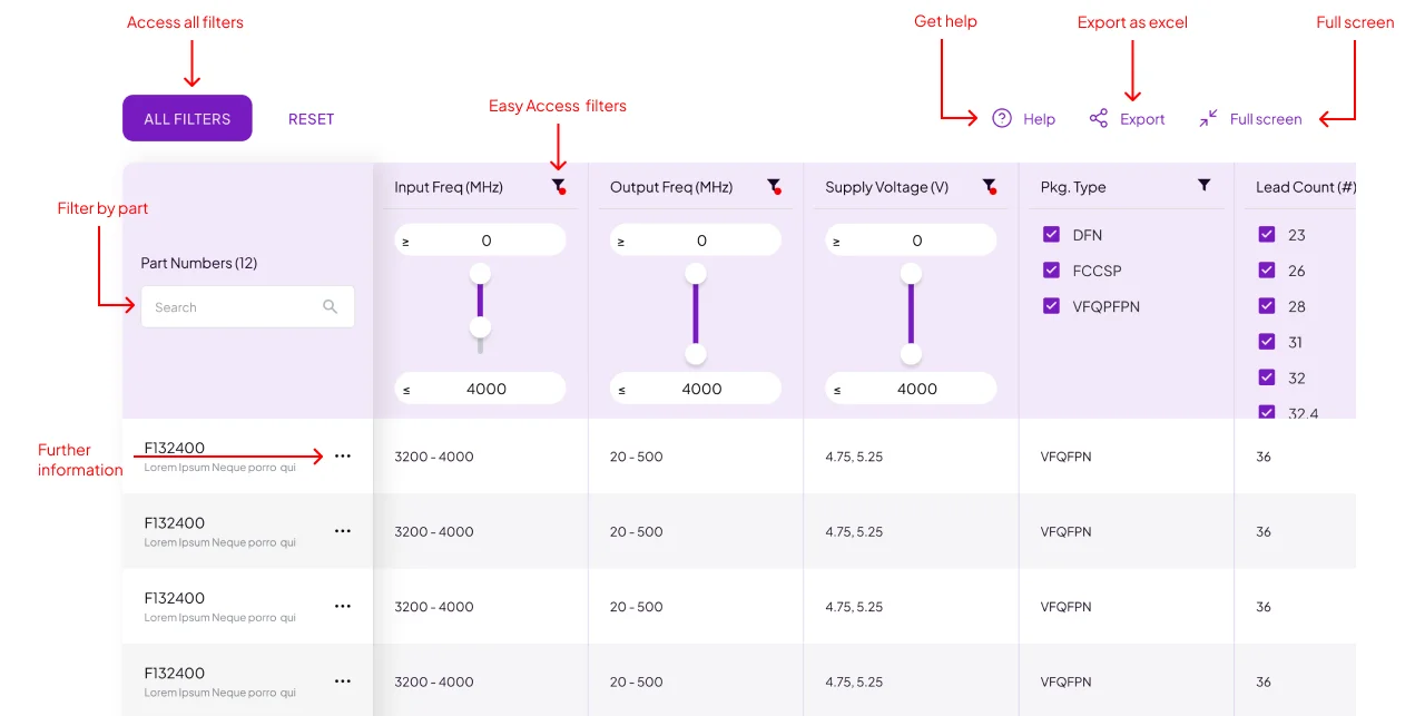
Product Details

- Gain at 3500MHz
- 35dB typical in High Gain Mode
- 29dB typical in Low Gain Mode
- 1.35dB NF at 3500MHz
- +23dBm OIP3 at 3500MHz
- OP1dB at 3500MHz
- +15dBm in High Gain Mode
- +14dBm in Low Gain Mode
- 50Ω single-ended input/output amplifier impedances
- IDD = 130mA
- Independent Standby Mode for power savings
- Supply voltage: +3.15V to +3.45V
- 6mm × 6 mm, 32-pin LGA package
- -40 °C to +105 °C exposed pad operating temperature range
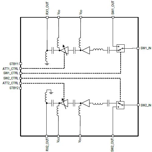
The F0453C is an integrated dual-path RF front-end consisting of an RF switch and two gain stages with 6dB gain control used in the analog front-end receiver of an Active Antenna System (AAS).
The F0453C provides 35dB gain with +23dBm OIP3, +15dBm output P1dB, and 1.35dB noise figure at 3500MHz. Gain is reduced 6dB in a single step with a maximum gain settling time of 31ns. The device uses a single 3.3V supply and 130mA of IDD.
The F0453C is offered in a 6mm × 6mm × 0.8mm, 32-pin LGA package with 50Ω input and output amplifier impedances for ease of integration into the signal path.
Design & Development (Boards and Kit)
.png)
Evaluation Board for F0453C RF DVGA
The F0453CEVB is a fully populated test board enabling easy evaluation of the F0453C RF Switch / LNA performance.
Part Numbers (2)
F0453CLFGK
F0453CLFGK8
Do you have more questions?
We're here to help you explore possibilities, optimize performance, and drive technological advancements. Reach out today!
Talk to Sales